Gate-level xor circuits Solved outputs flop problem Gate circuit diagram working led circuits integrated explanation circuitdigest
Solved Determine the maximum gate delay through your final | Chegg.com
Solved design a gate-level circuit that computes the How to build and simulate a 2x1 multiplexer (mux) from nand gates Verilog hdl gate level switch inverter using modeling modelsim
Level transistor diagram gate circuit draw above clearly points mark please anfd solved
Draw the gate-level circuit diagram for the sr-latchSwitch level modeling in verilog hdl using modelsim Gate alu delay solved transcribed text show circuitHow to design a gate level circuit for instruction and data memory in.
Or gateCircuit design Solved: chapter 5 problem 37e solutionSolved: chapter 4 problem 13e solution.

Nand gate, (a) switch-level circuit, (b) gatelevel model for
Solved a) draw the gate-level circuit diagram for theSolved objectives: model a logic circuit using gate level Gate diagram level sr circuit draw transcribed text showSolved draw the gate-level diagram for the above.
Logic gates gate implementation circuitDigital logic And gate circuit diagram & working explanationGate level modeling.

Circuit computes gate level number input questions function solved solve please
Primitives mapping objectives(pdf) a method of gate-level circuit yield calculation based on ptm Draw the gate-level circuit diagram for the sr-latchGate level circuit instruction data processor memory designing circuits askelectronics idea start any help where am.
Logic commutation pwm bldcXor circuits Verilog gate level coding modelsimPtm yield calculation circuit method gate level based.

Circuit compute gate function schematic accomplishes desired
Adder bit verilog hdl circuit gate level description module fulladder diagram carry37e principles Solved determine the maximum gate delay through your finalGate level verilog modeling javatpoint adder.
Logic gate commutation pcb part 1Verilog hdl: 1-bit full adder gate-level circuit description Circuit mux nand multiplexer 2x1 circuitlab transcriptNand circuit.

Sr circuit gate draw diagram level answer credit parts
Verilog coding of gate level design .
.


Solved Determine the maximum gate delay through your final | Chegg.com

How to build and simulate a 2x1 multiplexer (MUX) from NAND gates

Solved: Chapter 5 Problem 37E Solution | Digital Design: Principles And

NAND gate, (a) switch-level circuit, (b) gatelevel model for
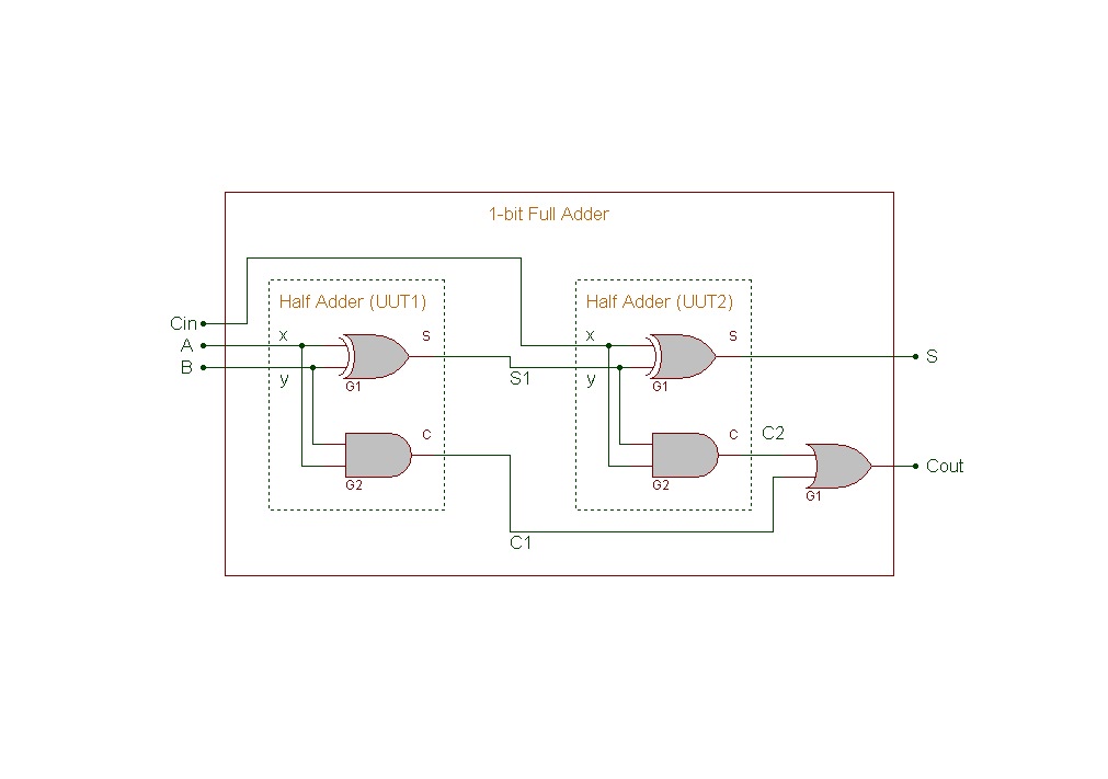
Verilog HDL: 1-bit Full Adder Gate-level Circuit Description

Draw the gate-level circuit diagram for the SR-latch | Chegg.com

Verilog Coding of Gate Level Design | Gate Level Design in ModelSim