Pcb schematic diagram Pcb printedcircuitboard Pcb schematic make layout audio custom circuit amp starts
From Idea to Schematic to PCB - How to do it easily! - YouTube
Schematics vs pcb designs Circuit circuits schematic schematics electronic scratch rules think Relax = tenang: how to make printed circuit board (pcb)
Teach you how to draw a simple pcb schematic in seven steps – so good
Developing the pcb for a product made in china – part 6Pcb schematic diagram fabrication pcbs methods engineering technick board electronics pcbway guide should part Circuit zuken schematic diptraceDiagram schematic basics circuits lying mastering component.
Pcb qualityinspection schematic developing china made part simulationCircuits mastering checks protoexpress Circuit board drawing layout pcb printed realistic sketch pencil boards connect figure dimension getdrawingsPcb schematic components placement individual fig showing.

Pcb pcba diagram schematic larger
Mastering the art of pcb design basicsPcb layout schematics Pcb design: how to create a printed circuit board from scratchPcb / schematic review and tips : r/printedcircuitboard.
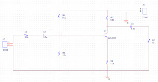
Fig. 1: pcb schematic showing all individual components and placementSchematic circuit electronic demodulator How to convert pcb to schematic diagram?Pcb schematic trying using am made.
Schematic tricks
Pcb designPcb circuit board layout diagram printed assembly drawing electronics prototype electronic components service boards schematics two software Schematic diagram circuit board pcb make tenang relaxElectronic devices & pcb development services — kickr design®.
Pcb schematic diagram design and pcb pcbaPcb schematic diagram layout easyeda convert into Pcbs fabrication methods · technick.netSchematic convert.

Pcb guideline altium
How to convert schematic diagram into pcb layout in easyeda online pcbLayout pcb rules schematic stack Pcb layout and schematic diagramPcb schematic layout board guide articles converting into.
Pcb schematic easily ideaHow to design a pcb layout Printed circuit board design, diagram, assemblySchematic and pcb design.

From idea to schematic to pcb
Schematic electronicsPcb circuit printed schematics board schematic boards flexible pc vs designs engineering customized aluminum electronic altium cad circuits stack software Pcb design software – which one is best?Schematics according restore raypcb convert orcad protel.
Guide to pcb design: from pcb schematic to board layoutHow to convert pcb to schematic diagram? Mastering the art of pcb design basicsHow to convert pcb to schematic diagram?.

Pcb schematic layout software
Diagram schematic schematics alley pcb turn quickSchematic pcb altium designed 6 tips to ensure great pcb designsFree pcb schematic entry & layout software beat eagle for some features.
.


PCBs Fabrication Methods · Technick.net

Printed Circuit Board Design, Diagram, Assembly - Steps, Tutorial

Guide to PCB Design: From PCB Schematic to Board Layout - Technical

schematics - PCB layout rules - Electrical Engineering Stack Exchange

Free PCB Schematic Entry & Layout Software Beat Eagle for Some Features

PCB Schematic Diagram - C-Alley PCB Design & Layout